The Cornerstone of the Digital Universe: Transistor Wars, the Rise of AI, and the Future of Technology
The evolution of transistors at the heart of the modern digital world: TSMC's pure-play foundry model, Moore's Law, and GAAFET nanosheet architectures.
Greetings, and welcome to my first blog post. I plan to share articles here periodically; if you would like me to launch a newsletter, feel free to reach out.
Introduction: The Power of the Invisible Engine
From the smartphone in our pocket to the laptop on our desk and the cloud data centers around the globe, the technology powering every moment of modern life can feel like abstract magic. While browsing on a device equipped with Apple’s M4 processor or marveling at an artificial intelligence application accelerated by Nvidia’s latest GPU, it is easy to overlook the physical source of that power.
Yet beneath all these digital experiences lies an invisible engine tens of thousands of times smaller than a strand of human hair: the transistor. These microscopic switches are the fundamental building blocks of the digital revolution and sustain the entirety of modern electronics. Inside an Apple M4 chip, for instance, 28 billion transistors switch on and off trillions of times per second to execute our instructions.
 Figure: Processors at the heart of the digital world.
What Exactly Is TSMC?
Founded by Morris Chang in 1987, the Taiwan Semiconductor Manufacturing Company (TSMC) revolutionized the technology industry by inventing the “pure-play foundry” business model.
Designers vs. Manufacturers
We can illustrate this model with a clear analogy:
- Designers (Fabless): Companies like Apple, Nvidia, AMD, and Qualcomm are like world-class architects. They design every detail of a chip but do not own fabrication plants.
- Manufacturer (Foundry): TSMC is the world’s most advanced construction firm. It takes Apple’s blueprint and turns it into physical silicon.
TSMC is called a “pure-play” foundry because it never designs or sells chips under its own brand; its sole mission is to manufacture its customers’ designs using leading-edge lithography. This allows tech giants to focus on architecture without bearing the tens of billions of dollars required to build semiconductor fabs.
Moore’s Law: The Industry’s Self-Fulfilling Prophecy
Although often spoken of as a law of physics, Moore’s Law is in fact a powerful economic and industrial observation. Proposed in 1965 by Intel co-founder Gordon Moore, it posits that the number of transistors on a chip doubles roughly every two years.
The Economic Engine and Existential Limits
- Cost Reduction: The law predicted not only rising compute density but also a steep drop in cost per transistor—igniting the economic engine that brought computing out of laboratories and into our pockets.
- Self-Fulfilling Roadmap: Because the entire semiconductor ecosystem believed in this cadence, billions of dollars in R&D were coordinated around it, turning the observation into reality.
- Atomic Boundaries: Today we are approaching the physical limits of silicon at the atomic scale. Slowing scaling forces the industry to rethink the economic model built on annual generational leaps.
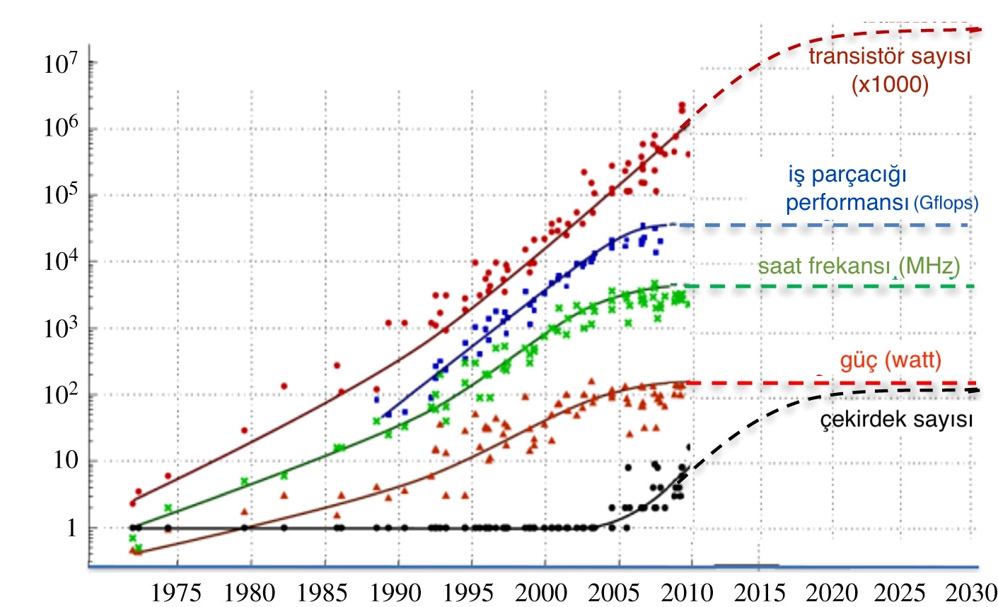 Trends in transistor count ($10^{7}$), single-thread performance, and power consumption.
Dancing at the Atomic Limit: Evolution of Transistor Architecture
To keep Moore’s Law alive, transistors had to evolve from two-dimensional planar structures to three-dimensional gate architectures.
| Technology | Architecture | Key Advantage | Primary Limitation |
|---|---|---|---|
| Planar FET | 2D (Gate on top) | Baseline control | High current leakage at small nodes |
| FinFET | 3D (Gate wraps 3 sides of fin) | Improved electrostatic control | Limited control below 5 nm |
| GAAFET (Nanosheet) | 3D (Gate surrounds all 4 sides) | Superior electrostatic control | Extreme manufacturing complexity |
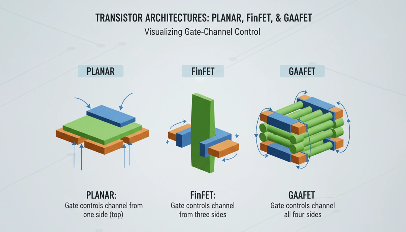 Figure: Structural comparison of Planar FET, FinFET, and GAAFET.
Summary
Transistors—the bedrock of our digital universe—are not merely electronic components; they are the economic engine shaping the global technology landscape. Despite quantum and atomic constraints, the transition from Planar to FinFET and now GAAFET continues to push the boundaries of physics.
Author: Kerem Uysal
Contact: info@keremuysal.com